Called EPC2055 it is a “good example of the rapid evolution of GaN FET technology”, according to company founder and CEO According to Alex Lidow. This 40 volt device offers both smaller size and reduced parasitics compared with previous-generation 40 V GaN FETs and at lower cost.”
Although GaN power transistors which are HEMTs, have no inherent avalanche capability, the device is rated to handle up to 10,000 5ms pulses to 48V.
Continuous current rating is 29A, with short pulses to 161A, while packaging is 2.5 x 1.5mm chip-scale with a junction to board thermal resistance of 2.5°C/W and operation is across -40 to 150°C.
Drain-source on-resistance is measured at 15A with 5V on the gate, which has a nominal forward leakage (the gate is a diode) of 10μA typ (800μA max), rising to 100μA typ (5mA max) at 125°C. Absolute max gate excursions are +6V and -4V with respect to the source – so great care is needed to keep transients out of the gate drive, something that should not put designers off if they are prepared to master the details.
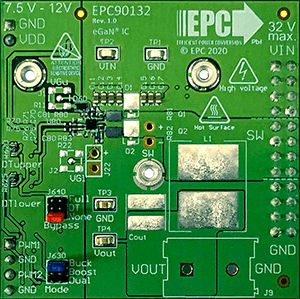
 To help with design-in, the EPC90132 development board (left) features the transistor in a 40Vmax in, 25A max out, half-bridge boost or buck power stage.
The ~50 x 50mm PCB has two EPC2055 with a uP1966A gate driver from uPI Semiconductor, as well as a 100V 2.8Ω EPC2038 in a synchronous bootstrap circuit – which is worth a look in itself, as is the use of 74LVC1G99G multi-function gates in the dead-time circuits.
“To simplify the evaluation process, all the critical components and layout for optimal switching performance are implemented,” according to EPC, which has also created a video called ‘How to turn a development board into a working prototype‘ (slow start, useful detail later).
Other applications foreseen for the transistor are LED lighting, 12 – 24V input motor drivers and lidar systems for robotics, drone and autonomous cars, according to the company.
